プリント基板をPress-n-Peelで作製する. 20th Aug.2021 Yoshio Okamoto
Making printed circuit boards using Press-n-Peel sheets.
Press-n-PeelはAmazonなどで買えます.
You can buy Press-n-Peel at Amazon or other net shops.
下記のサイトも製作の参考になります.(Reference site; Japanese only)
https://minoyalab.com/electronic-work/transfer-sheet-pcb.html
<ここでは自作地震計用の3ch増幅回路基板を例にとる>
This circuit is a 3ch amplifier for our hand-made seismographs.
1.基板パターンの印刷(Laser Printing of circuit patterns)
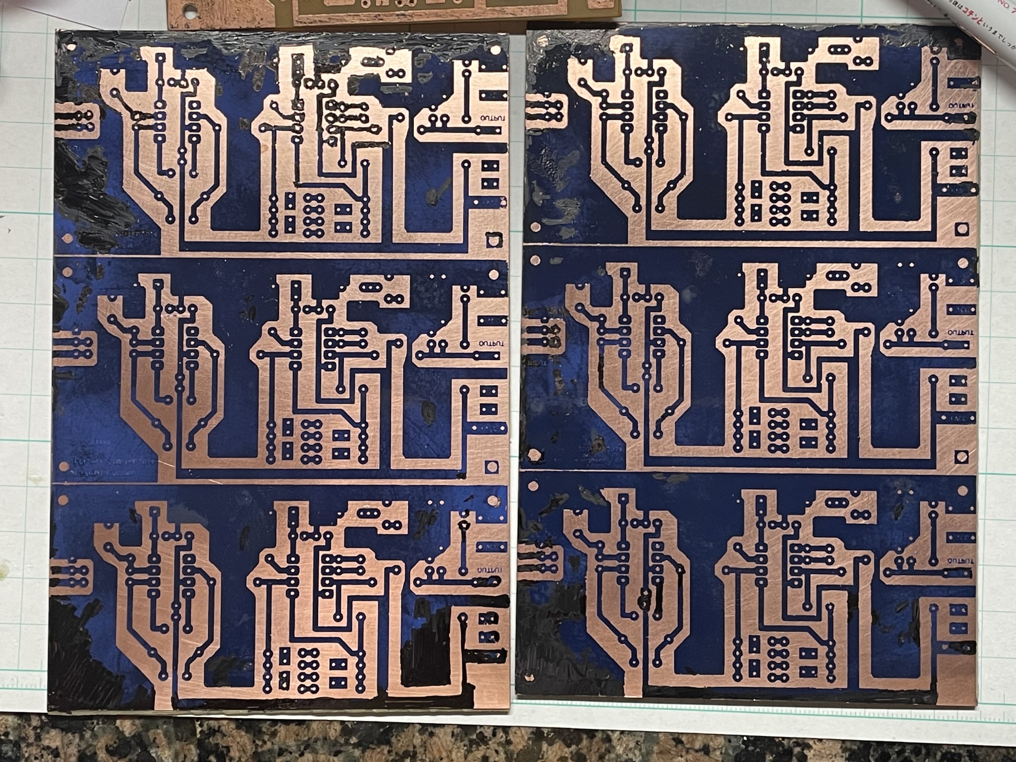
レーザプリンタで,基板図をPress-n-Peelに印刷する.必ずトナーを使うのが重要.また図は部品面から見た図であることに注意.なぜなら次の熱転写により裏返される.
Print the circuit pattern on the Press-n-Peel with black toner using a
laser printer. The schematic pattern is from parts side, not bottom
side.
Because the pattern is reversed at the next transfer stage.
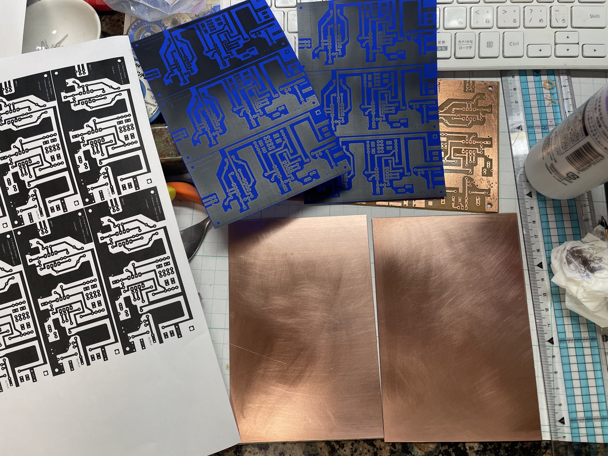
Upside center: printed on Press-n-Peel
Bottom center: raw circuit boards
2.熱転写(Thermal printing)
アイロンでシートのトナーを基板上に熱転写する.
Toner pattern is thermal transferred on a raw circuit board using an iron.
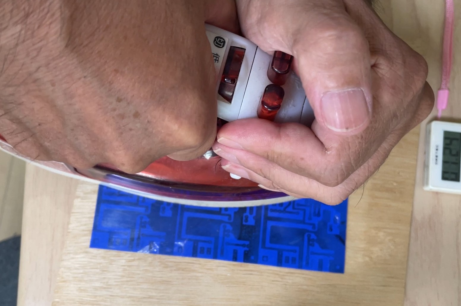
Strong pressure is need.
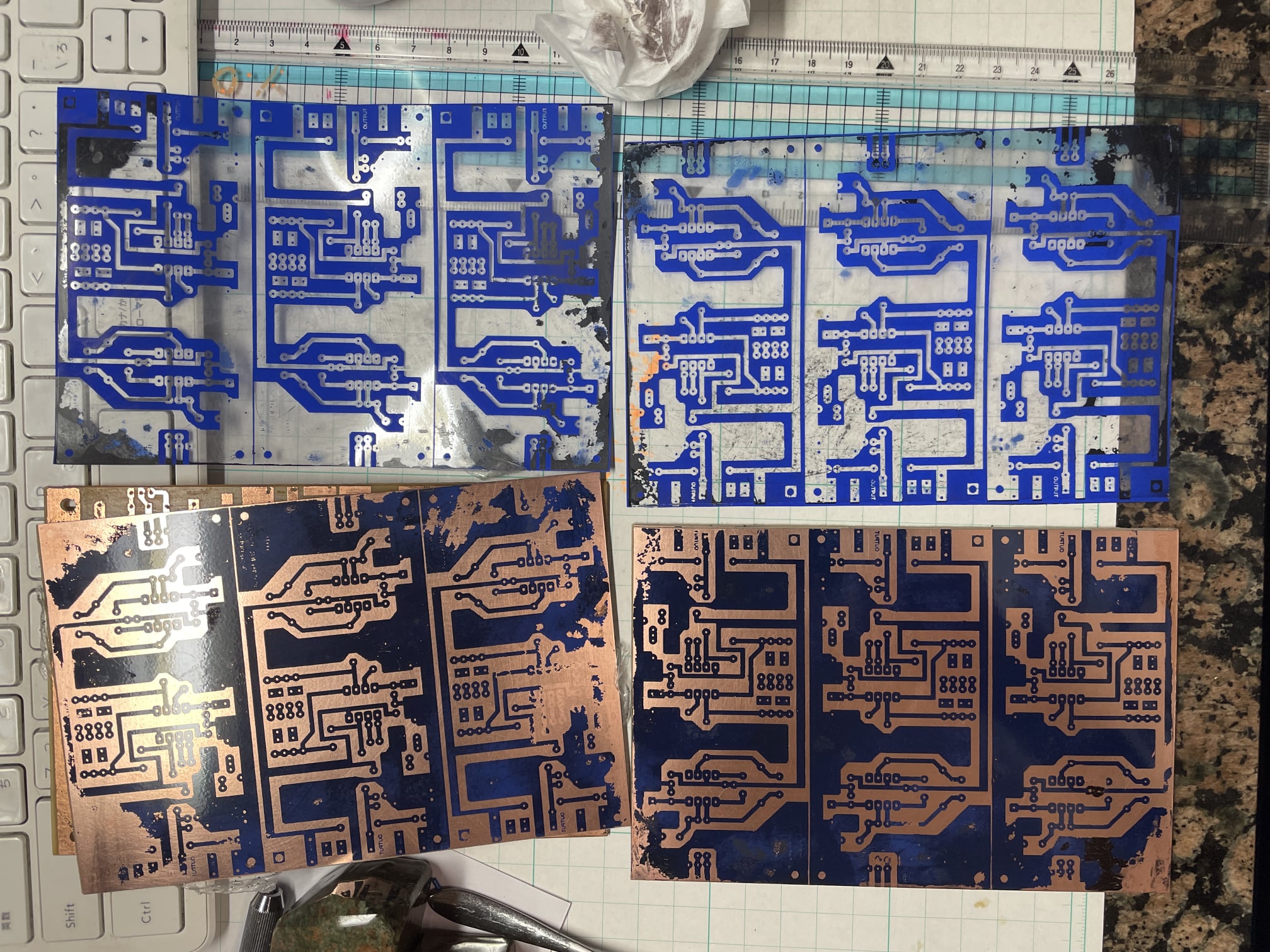
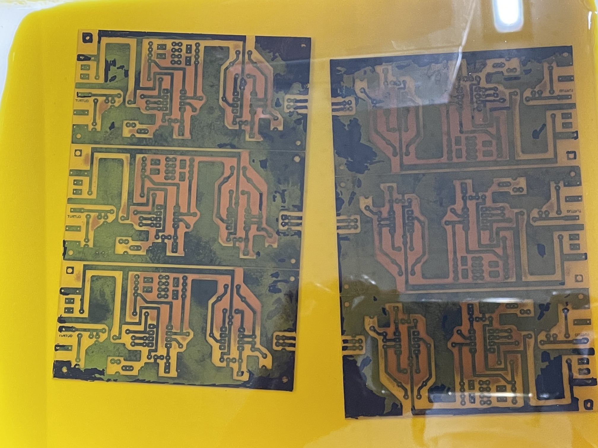
部分的に転写できていない箇所がある.
The process is not completed at some areas.
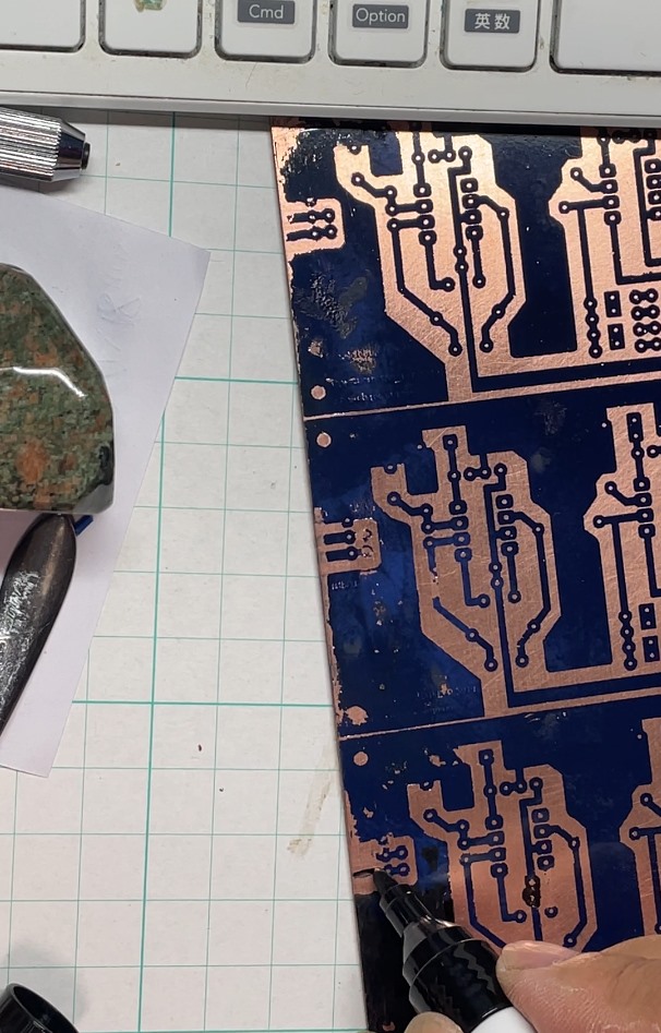
転写が失敗したパターンをあとて油性マジックペンで,書き足す.マジックの塗料を塗り重ねること.薄いとエッチング時に銅箔が溶ける.
Missing patterns are corrected using a oilier felt pen. Make thick layer
of paint, or the copper cover will be solute at the etching
process.
パターン修正終了.
Completed fixing patterns.
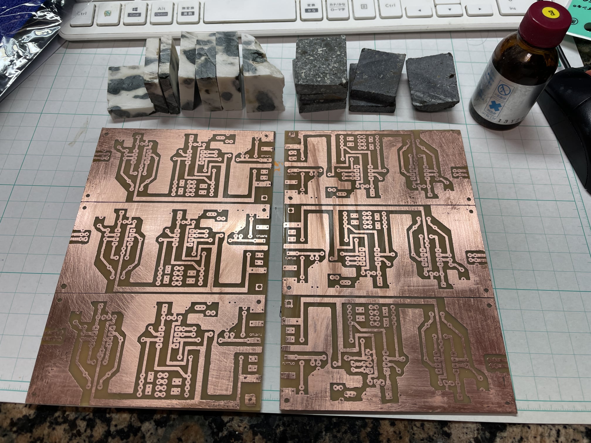
2.エッチング(etching)
塩化第二鉄溶液 Ferric chloride aqua(20-30%)40-50℃ を用意して,その中に基板を10分から20分浸す.露出した部分の銅箔がすべて溶けだせば終了.
Prepare ferric chloride aqua(20-30%)40-50℃, and soak the boards for 10
to 20 minutes until the all exposed copper foils are solute.
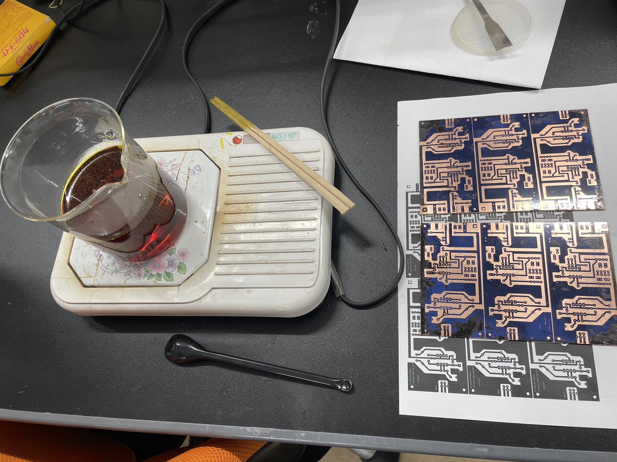
エッチング溶液の準備.塩化第ニ鉄90gを水300mlに溶かした.
Preparation of solution aqua. Ferric chloride 90g with 300ml water.
Keep 40-50℃ in the water bath until all exposed copper foils are solute.
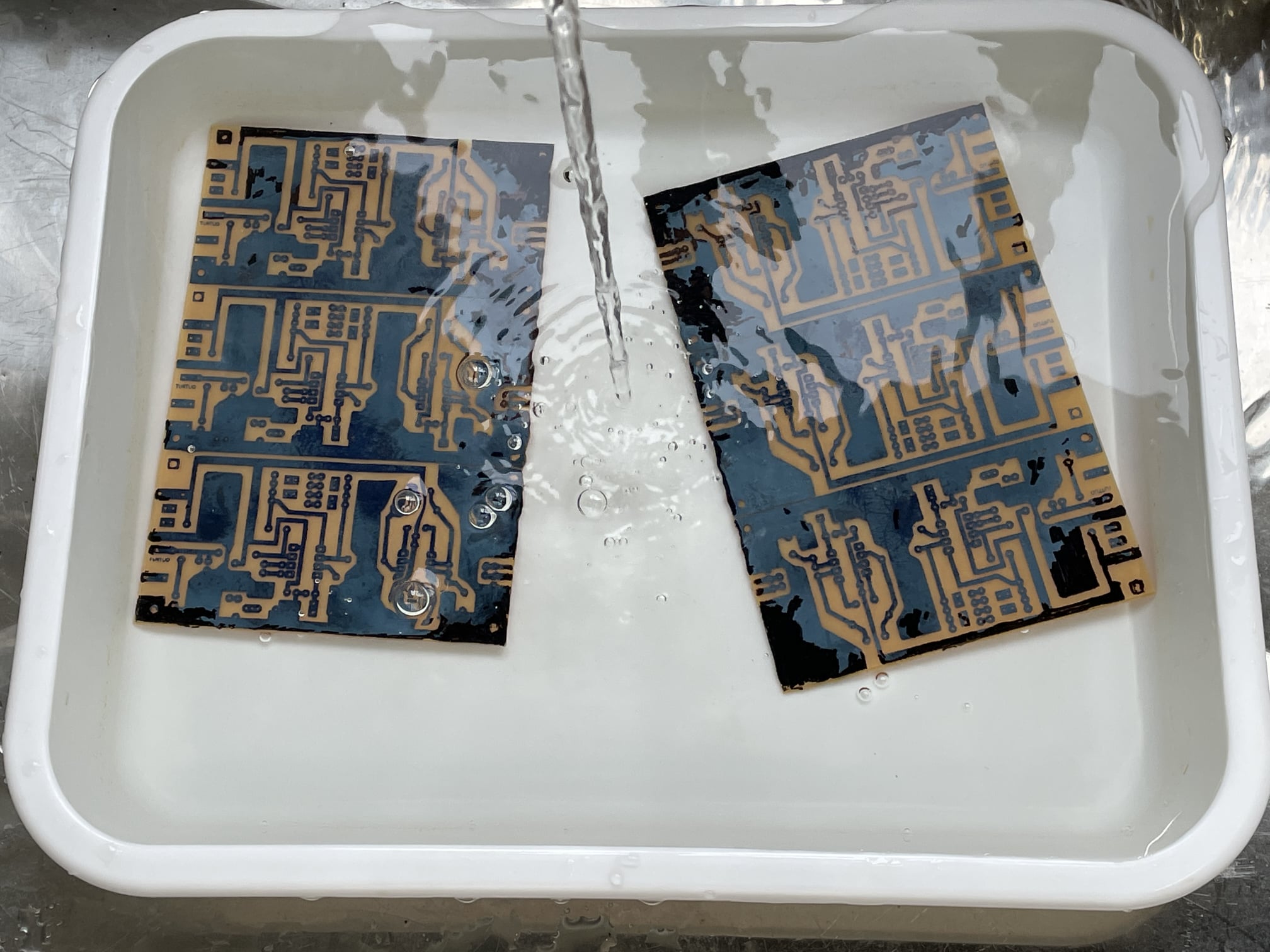
Washing under running water.
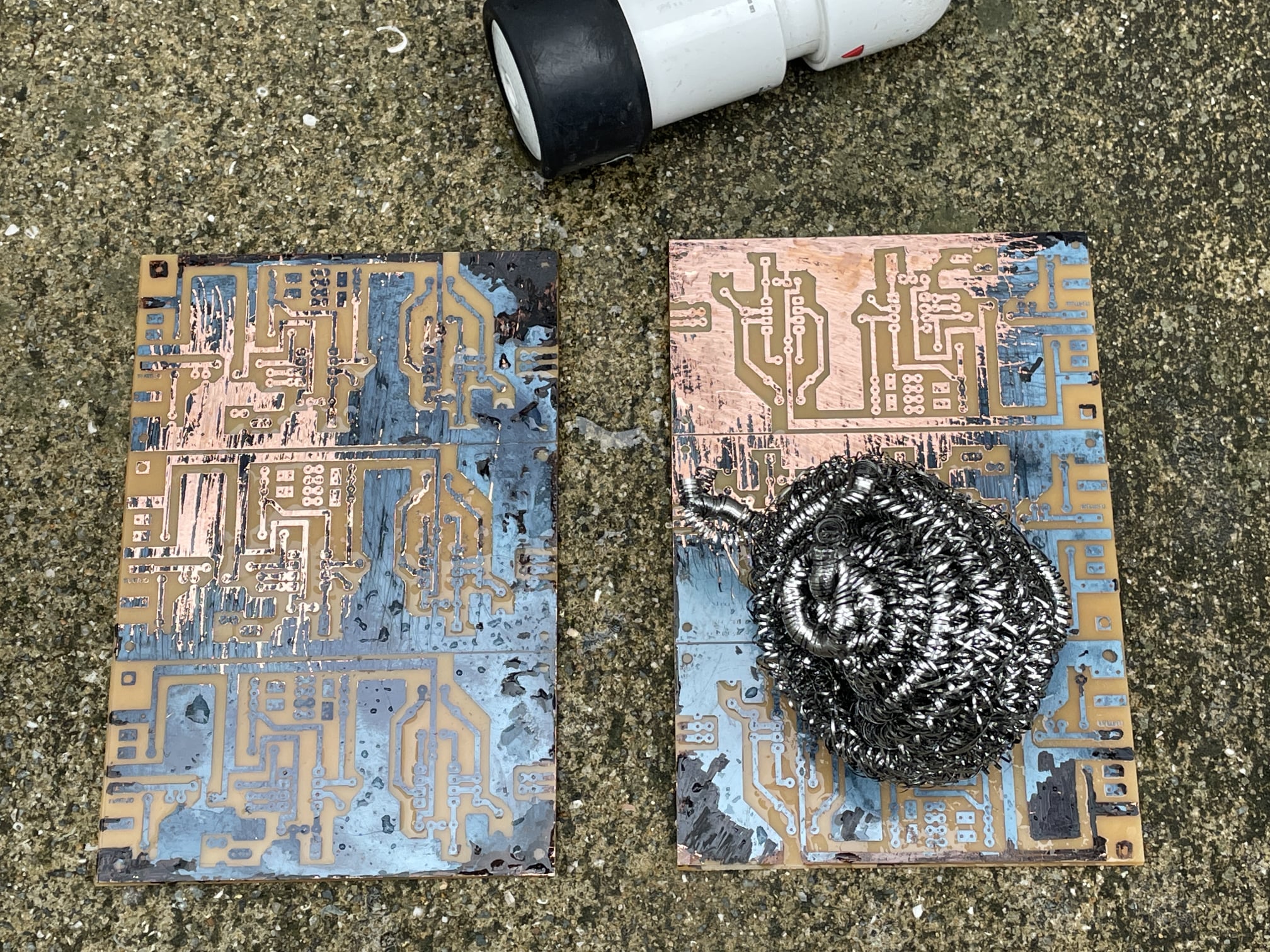
Remove the toner and film with a stainless scrubber.
Paint flux on the surface to prevent rusting.
4.穴あけ(Drilling)
直径1mmのドリルで穴を開ける.
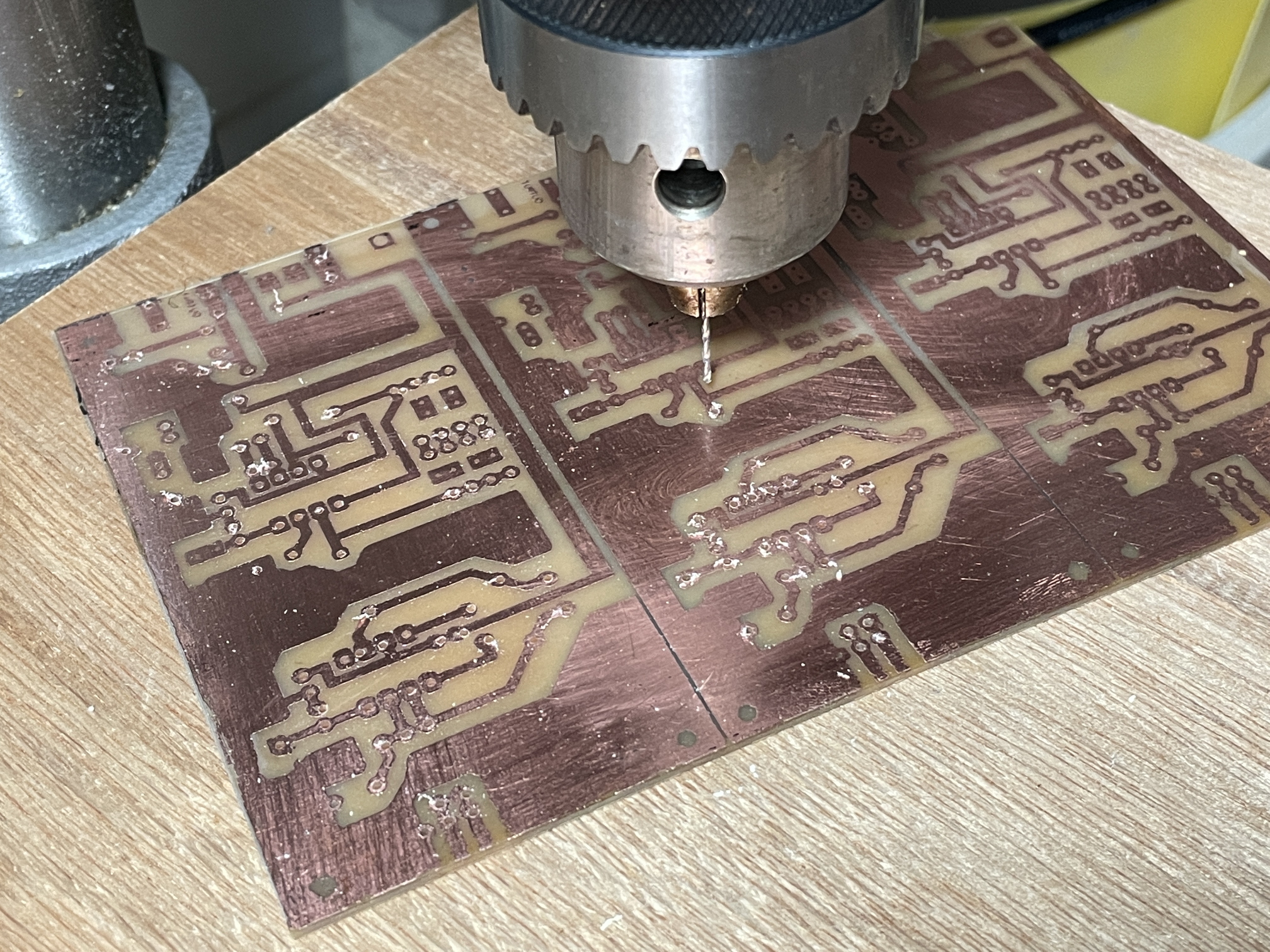
Drilling 1mm holes.
Copyright(c) by Y.Okamoto 2021, All rights reserved.